
One exciting thing about FPGAs is that when you program them, you are physically creating the digital circuits needed to execute your program. In effect, they “become” the hardware you’re trying to build. In this article, we’ll move past blinking LEDs to make something a bit more complex: hardware that talks to an ultrasonic sensor, measures the distance to a subject, and displays the distance on an LED display unit. But perhaps more importantly, you’ll create digital logic inside the iCE40 FPGA which reads the measurement from the ultrasonic sensor and displays that measurement on the LED.
As you build this project you’ll learn how to:
- Design digital hardware
- Work with Verilog syntax
- Build state machines and counters
- Use edge detection
- Measure pulse widths
- Use a clever algorithm to convert binary to BCD
- Drive a seven-segment LED display — the sort used in digital clocks
Requirements
- Lattice iCE40UP5K breakout board or equivalent
- Ultrasonic sensor HC-SR04
- Four-digit common cathode seven-segment display
- Breadboards and connecting wires
- 5V power supply for the ultrasonic sensor
Hardware Design
The high-level block diagram in Figure 1 shows our build.
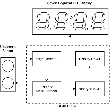 Figure 1: High Level Block Diagram
The ultrasonic sensor shown at left broadcasts an ultrasonic signal and measures the response from nearby objects. The sensor encodes the distance in a signal that is sent to the FPGA. The FPGA uses the edge detector and distance measurement unit to convert this signal to a distance value. The Binary to BCD (Binary Coded Decimal) module converts this data to a format suitable for the seven-segment LED display. The display driver is responsible for sending the BCD data to the display.
We’ll implement the edge detector, distance measurement, binary-to-BCD, display driver, and other required modules using Verilog.
Measuring the Distance
This project uses the popular and inexpensive ultrasonic sensor HC-SR04, shown below.
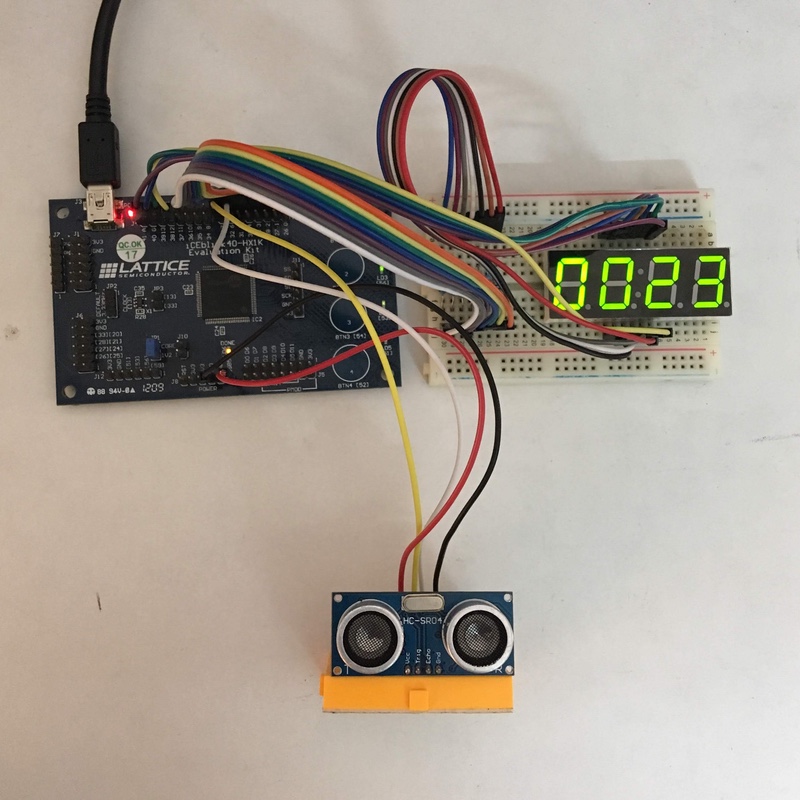 Figure 2: HC-SR04
As you can see, the HC-SR04 has four pins: VCC, Trigger (Trig), Echo, and Ground (GND). Figure 3 shows its timing diagram.
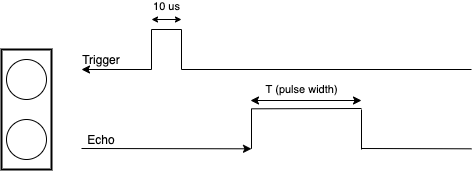 Figure 3: HC-SR04 timing diagram
In order to get distance information from this sensor we send a 10 microsecond HIGH pulse on the Trigger pin, which makes the sensor send a burst of ultrasound waves using its transmitting (T) ultrasonic transducer. These waves are reflected off objects and return to the receiving (R) transducer.
The sensor responds to received waves with a pulse on the Echo pin. The width of this Echo pulse represents the number of microseconds the sound waves take to travel from the transmitting transducer to the object and back to the receiving transducer. Hence, we compute the sensor’s distance to the object as follows, where D is the measured distance:
D = (pulse width in us) * 10^-6 * (speed of sound) / 2
Using 340 m/s as the speed of sound this works out to:
D (cm) = pulse width / 58
Since the range of the HC-SR04 is from 2 to 400 cm we measure the distance in centimeters.
The State Machine
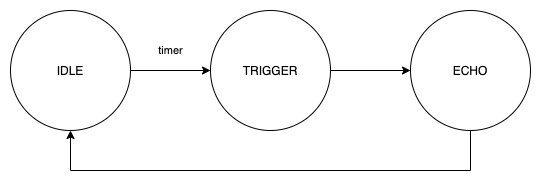 Figure 4: Ultrasonic sensor measurement state machine
The system starts in the IDLE state then moves into the TRIGGER state after a preset time. It remains in the TRIGGER state until a pulse is sent. Now it shifts to the ECHO state where it awaits the reflected pulse and measures its width. Finally, it returns to IDLE.
The Distance Measurement
Listing 2.1 shows how to implement this distance measurement in Verilog by defining both counters (a common way to create periodic events in an FPGA) and the state machine.
// from ultrasonic.v
// clk is at 12 MHz
reg [21:0] counter;
reg [7:0] trig_counter;
reg [21:0] npulses;
reg [13:0] distance;
assign w_distance = distance;

// pulse parameters
parameter T1 = 8'd120;

// state machine
parameter sIDLE    = 2'b00;
parameter sTRIGGER = 2'b01;
parameter sECHO    = 2'b10;

reg [1:0] state;
Listing 2.1
First we declare the counters. Our board has a clock speed of 12 MHz. Reading top to bottom, counter is a 22-bit value which overflows at 2²² − 1 = 4,194,303. If we increment the count on every positive edge of the clock tick, the overflow will happen approximately every 0.35 seconds: 4194303 / 12000000. Similarly, trig_counter overflows approximately every 10 microseconds — which is what we need to generate the trigger pulse.
We use the npulses variable to track the incoming pulse width. The distance variable stores the computed distance in centimeters. The constant parameter T1 generates the correct trigger pulse width by comparing it with trig_counter.
The three states are defined as a series of two-bit Verilog parameters (since we have only three states): sIDLE, sTRIGGER, and sECHO. The state variable keeps track of the current state of the system.
Coding the Edge Detector
We use the edge detector to detect the start and end of the received signal, or incoming echo pulse. Listing 2.2 shows how it’s declared.
// edge detector
wire pos;
wire neg;
edge_detect ed1 (
    .clk(clk),
    .sig(echo),
    .pos(pos),
    .neg(neg)
);
Listing 2.2
Creating the Trigger Pulse
Let’s look at the state machine code to see how we create the trigger pulse. For the sake of simplicity we’ll analyze one state at a time, beginning with TRIGGER as shown in Listing 2.3.
always @(posedge clk) block of the code.
We begin with a “reset” signal that sets the counters to zero and the state to IDLE. This is good practice as it ensures that the variables do not already contain values that might skew our results.
// from ultrasonic.v
// reset variables
if (!resetn)
begin
    trig_counter <= 0;
    state        <= sIDLE;
    counter      <= 0;
    npulses      <= 0;
end
// increment counter
counter <= counter + 1;
Listing 2.3
The signal is named resetn to indicate that it is active-low; in other words the reset happens when the signal goes LOW. For every positive edge of the clock, we also increment counter.
Handling Changes in State
Listing 2.4 shows how we handle changes in the state machine.
case (state)
    sIDLE:
    begin
        // when counter overflows, send a trigger
        if (!counter)
        begin
            state <= sTRIGGER;
        end
    end
Listing 2.4
The case statement checks the current state of the state machine and executes the appropriate code. When in IDLE and counter overflows, we switch to the TRIGGER state.
Listing 2.5 shows what happens in the TRIGGER state.
    sTRIGGER:
    begin
        trig_counter <= trig_counter + 1;
        if (trig_counter == T1)
        begin
            // go to echo
            state        <= sECHO;
            // reset the count
            trig_counter <= 0;
        end
    end
Listing 2.5
trig_counter is incremented at every clock. When the counter reaches the value of T1, we change the state to ECHO and reset the counter to zero, as a result of this continuous assignment statement that follows the always block:
// set trigger state
assign trig = (state == sTRIGGER);
The above is known as a continuous assignment statement in Verilog, which means the output changes as soon as the values on the right of the equal sign change. The trig variable is high only when we are in TRIGGER state — low to begin with, and as soon as we exit TRIGGER it becomes low again. This is how we create the trigger pulse for the ultrasonic sensor!
Coding the Distance Computation
The ECHO state is where the distance computation happens. Listing 2.6 shows the code.
    sECHO:
    begin
        // count pulses
        npulses <= npulses + 1;

        // start of echo
        if (pos)
        begin
            npulses <= 0;
        end

        // end of echo
        if (neg)
        begin
            // dt = 1/f
            // t = n*(1/f)*10^6 us
            // d = n*(1/f)*10^6 / 58 cm
            // f = 12 MHz
            // d = N/(12*58) ~ N/696
            // N/696 = N * (65536/696) / 65536 = N*94 >> 16
            distance <= (npulses*94) >> 16;
            state    <= sIDLE;
        end

        // avoid getting stuck here
        // check max distance 400 cm = 696*400 = 278400
        if (npulses > 300000)
        begin
            npulses <= 0;
            state   <= sIDLE;
        end
    end
Listing 2.6
We increment npulses to track the echo pulse width, resetting it to zero when the start of the pulse (low-to-high) is detected via pos. The end of the pulse is detected when it goes high-to-low, and neg becomes high.
The distance computation uses the formula:
D (cm) = pulse width in microseconds / 58
Since pulse width in microseconds = (number of pulses / clock frequency) × 10⁶, this works out to:
D = N / (12*58) ~ N / 696
  = N * (65536 / 696) / 65536
  = N*94 >> 16
The npulses > 300000 check ensures we don’t get stuck in the ECHO state if the ultrasonic sensor has a problem. 300,000 pulses at 12 MHz is well beyond the maximum valid distance the sensor can report (400 cm = ~278,400 pulses).
Displaying Digits on LED: The Binary to BCD Converter
To display the measured distance on the LED we use a mathematical method to extract the digits from the number. Listing 2.7 shows how to do that with Python.
>>> 1234
1234
>>> (1234) % 10
4
>>> (1234//10) % 10
3
>>> (1234//100) % 10
2
>>> (1234//1000) % 10
1
Listing 2.7
So, if we do truncated integer division (//) on a four-digit number by 10, and do modulo (%) 10 on it, we extract the tens digit. We can similarly extract each of the other digits. (Fire up a Python shell and try this on any 4-digit number of your choice!)
Unfortunately the above method is not ideal for FPGAs. Division and modulo operators take up a lot of resources to implement on FPGA fabric — our Verilog code maps to LUTs and other resources, and our goal is always to minimize resource usage. So instead of division and modulo, we will use another interesting method to extract the digits — one that uses only inexpensive operations such as shifts and additions.
The Double Dabble Algorithm
Before we get into details of this rather interestingly-named algorithm, let’s first look at BCD, or Binary Coded Decimal representation of numbers.
The binary representation of the decimal number 1234 is 010011010010. You can verify with Python:
>>> bin(1234)
'0b10011010010'
But 010011010010 is not useful if we are trying to show the digits 1, 2, 3 and 4 on a display. What we need is a representation where we get each decimal digit in binary. In that representation, 1234 would be 0001 0010 0011 0100. This is called Binary Coded Decimal or BCD, and is very useful for many situations — like sending each digit separately to a segmented display. So what we’re looking for is a way to convert the binary representation of our computed distance to BCD. That’s where the double dabble algorithm comes in.
The double dabble algorithm is simple to implement, yet tricky to understand, and is best illustrated with an example. Let’s try it with 1111011 which is the binary representation of 123. The table below shows how the algorithm proceeds via simple bit shifts and additions.
| 10² | 10¹ | 10⁰ | Original | Operation |
|---|---|---|---|---|
| 0000 | 0000 | 0000 | 1111011 | Initial values |
| 0000 | 0000 | 0001 | 1110110 | Shift Left (1) |
| 0000 | 0000 | 0011 | 1101100 | Shift Left (2) |
| 0000 | 0000 | 0111 | 1011000 | Shift Left (3) |
| 0000 | 0000 | 1010 | 1011000 | Add 3 to 10⁰ since value 0111 (7) > 4 → 1010 (10) |
| 0000 | 0001 | 0101 | 0110000 | Shift Left (4) |
| 0000 | 0001 | 1000 | 0110000 | Add 3 to 10⁰ since value 0101 (5) > 4 → 1000 (8) |
| 0000 | 0011 | 0000 | 1100000 | Shift Left (5) |
| 0000 | 0110 | 0001 | 1000000 | Shift Left (6) |
| 0000 | 1001 | 0001 | 1000000 | Add 3 to 10¹ since value 0110 (6) > 4 → 1001 (9) |
| 0001 | 0010 | 0011 | 0000000 | Shift Left (7) |
At the end of the process, we’ve ended up with 0001, 0010 and 0011 in the first three columns — the binary representations for the digits 1, 2, and 3 — just what we were aiming for!
I highly recommend the YouTube video by Computerphile for a deeper look at how this algorithm works: https://www.youtube.com/watch?v=eXIfZ1yKFlA
Verilog Implementation of Double Dabble
State machines are a common way to implement complex logic in an FPGA. Let’s look at the state machine for Double Dabble Binary to BCD conversion.
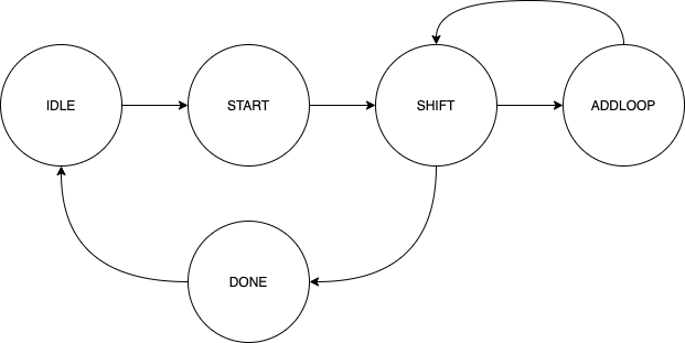 Figure 5: State machine for Double Dabble algorithm
Our state machine has 5 states — IDLE, START, SHIFT, ADDLOOP, and DONE. Now let’s look at the Verilog code.
Here’s how the states are defined:
// state machine
parameter sIDLE    = 3'b000;
parameter sSTART   = 3'b001;
parameter sSHIFT   = 3'b010;
parameter sADDLOOP = 3'b011;
parameter sDONE    = 3'b100;
We’re using 3-bit numbers to define states since we have only 5 states. (A 3-bit number can represent a maximum of 2³ = 8 states.) The state machine starts in the IDLE state:
reg [2:0] curr_state = 0;

always @ (posedge clk)
begin
    case (curr_state)
        sIDLE:
        begin
            if (start)
                curr_state <= sSTART;
        end
When the start signal is high, curr_state is set to START. Now let’s look at the START state:
        sSTART:
        begin
            // initialize
            buffer    <= value_bin;
            // change state
            curr_state <= sSHIFT;
            // set done
            reg_done  <= 0;
        end
buffer is initialized to the input value being converted to BCD. We set the current state to SHIFT and reset the reg_done flag. Remember that all three statements are happening in parallel — at the edge of the same clock. Remember to remove your microcontroller hat and put on your FPGA hat when looking at Verilog code!
This is what happens in the SHIFT state:
        sSHIFT:
        begin
            // shift 1 left
            buffer      <= buffer << 1;
            // keep track of shifts
            shift_count <= shift_count + 1;
            if (shift_count == (N-1))
                curr_state <= sDONE;
            else
            begin
                digit_index <= 0;
                curr_state  <= sADDLOOP;
            end
        end
We shift buffer to the left by one bit, as per the double dabble process. shift_count keeps track of the number of such shifts. We set the next state to DONE when we’ve completed N shifts (where N is the number of bits in the input). Otherwise we set the digit index to 0 and move to ADDLOOP.
Now let’s look at the ADDLOOP state, where the individual place digits are checked and 3 is added when a value exceeds 4:
        sADDLOOP:
        begin
            if (digit_index == (D-1))
                curr_state <= sSHIFT;
            else
            begin
                if (digit > 4)
                    buffer[N + 4*digit_index +: 4] <= digit + 3;
                digit_index <= digit_index + 1;
            end
        end
We set the state back to SHIFT once we’ve checked all the digits. We add 3 to the digit if its value exceeds 4, and increment the digit index to continue checking in the next clock cycle. The digit value comes from the following continuous assignment:
wire [3:0] digit;
assign digit = buffer[N + 4*digit_index +: 4];
This continuous assign statement extracts the required bits from an expression so it can be used inside an always block. Now let’s look at the DONE state:
        sDONE:
        begin
            // set idle state
            curr_state    <= sIDLE;
            // reset shift count
            shift_count   <= 0;
            // set done
            reg_done      <= 1;
            // copy bcd value
            reg_value_bcd <= buffer[N +: M];
        end
We set the next state to IDLE, reset the shift count, set the reg_done flag to 1, and extract our BCD result — the first M bits (least significant bits) of buffer using the Verilog slice operator +:.
Seven Segment Display
In this project, we will be using a Common Cathode four-digit seven-segment display.
The schematic for a typical display of this sort is shown in Figure 6 — from the manufacturer’s datasheet.
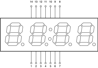 Figure 6: Schematic for common cathode 4-digit seven-segment display
The physical pin connections for such a display are shown in Figure 7.
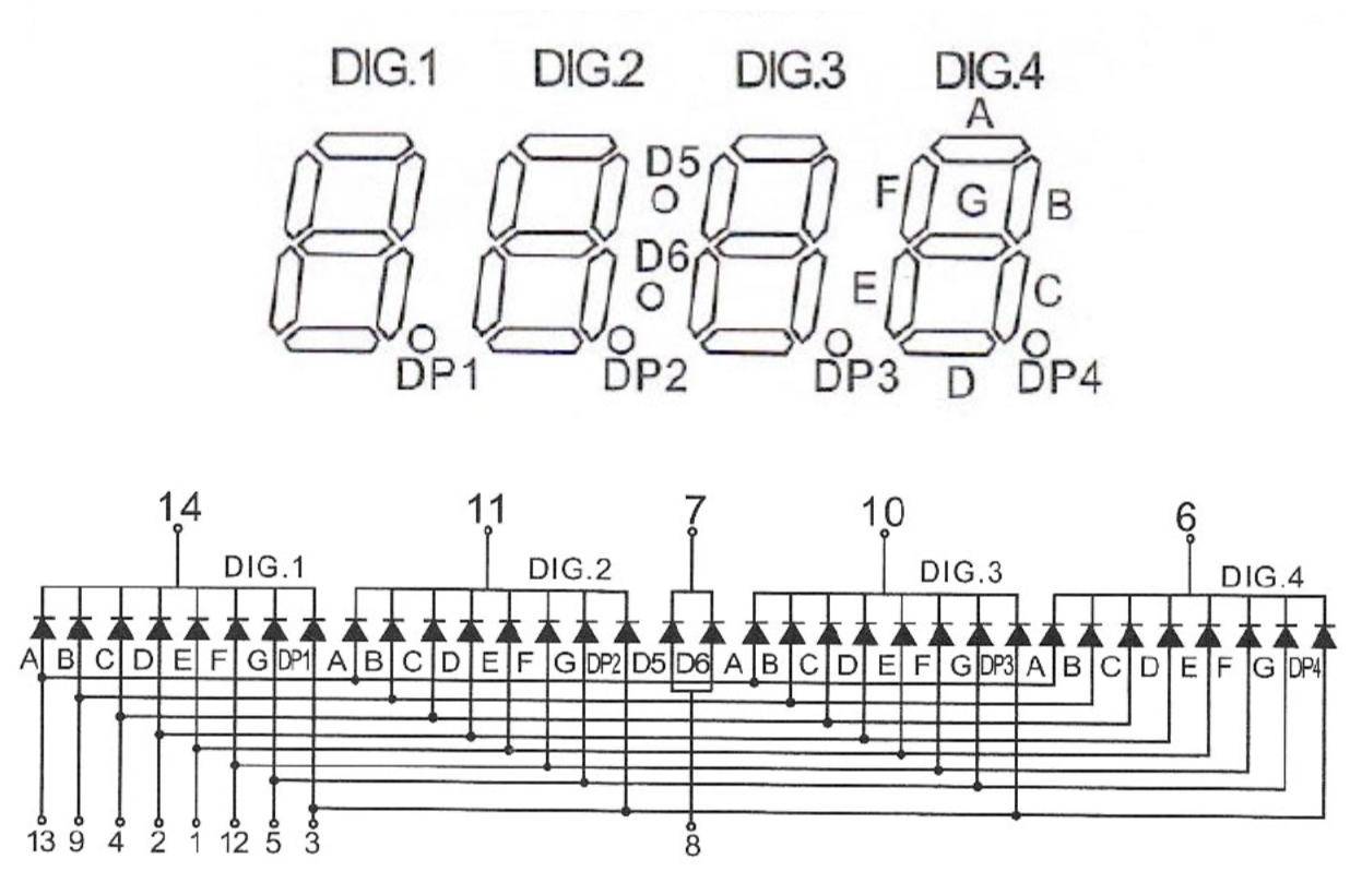 Figure 7: Pin connections for common cathode 4-digit seven-segment display
The display consists of four 7-segment digit units. Each digit has 7 LED segments named A through G that can be used to create digits, plus a decimal point DP. The display also includes two additional LEDs (D5 and D6) used to represent the colon (“:”) — traditionally used for displaying time. You display digits by lighting up specific sets of segments. For example, to display the digit 3, you would light up segments A, B, C, D, and G.
When we hook the display up to the FPGA, we add current limiting resistors to the anode lines. Even so, lighting up all LEDs of the display at the same time by directly connecting the GPIO pins of the FPGA to cathode lines will result in too much current and potentially damage the chip. So, to display 4 digits at a time, we use a trick that reduces power consumption: we light up one digit at a time and quickly cycle between the digits. Due to persistence of vision, it will appear as though all 4 digits are lit simultaneously.
Notice in Figure 6 how the anodes of a segment type (say A) of all digits are connected together? This means we need only 7 lines (excluding the decimal point) to control 4 digits. Each digit is switched on only when the corresponding cathode pin is grounded.
The code for the seven-segment display is in its own module seven_seg_cc_4d.v. Here’s how the module is defined:
module seven_seg_cc_4d(
    input clk,           // 12 MHz clock
    input  [19:0] value_bcd,  // a 4 digit BCD number
    output [3:0]  cathodes,   // 0 (enable), 1 (disable)
    output [6:0]  anodes      // Anodes - 7 lines
);
    reg [3:0] reg_cathodes;
    reg [6:0] reg_anodes;
    reg [3:0] curr_digit_value = 0;
    reg [1:0] curr_digit_index = 0;
The module takes as input the clk signal and a value in BCD format. The output cathodes is a 4-bit value used to enable or disable any of the 4 digits. Since grounding the cathode makes the LEDs light up, “enable” is 0. The output anodes controls the 7 segments in a digit. curr_digit_value is a 4-bit value ranging from 0 to 9, and curr_digit_index is a 2-bit value tracking the current digit (rightmost = 0).
Here’s how the mapping from digit value to anode bit pattern is done:
// digit to anode bits
always @ (*)
begin
    case (curr_digit_value)
        0: reg_anodes = 7'b1111110; // "0"
        1: reg_anodes = 7'b0110000; // "1"
        2: reg_anodes = 7'b1101101; // "2"
        3: reg_anodes = 7'b1111001; // "3"
        4: reg_anodes = 7'b0110011; // "4"
        5: reg_anodes = 7'b1011011; // "5"
        6: reg_anodes = 7'b1011111; // "6"
        7: reg_anodes = 7'b1110000; // "7"
        8: reg_anodes = 7'b1111111; // "8"
        9: reg_anodes = 7'b1111011; // "9"
        default: reg_anodes = 7'b1111110; // "0"
    endcase
end
The always @ (*) directive defines behavior that is not sensitive to any particular signal — a good way to assign register values continuously using a case statement. So for example, when curr_digit_value is 3, reg_anodes is set to 1111001. The 7-bit values correspond to segments A, B, C, D, E, F and G. 1111001 means: light up segments A, B, C, D, and G. From Figure 6 you can see this results in the digit ‘3’ being displayed.
Now let’s look at how data for a particular digit is extracted from the BCD value:
always @ (*)
begin
    reg_cathodes      = ~(4'b0001 << curr_digit_index);
    curr_digit_value  = value_bcd[4*curr_digit_index +: 4];
end
curr_digit_index is used to form the correct cathode bit pattern. For example, when curr_digit_index is 2, we get ~(4'b0001 << 2) = ~(4'b0100) = 4'b1011. This indicates which cathode should be grounded, enabling the corresponding digit. The current digit value is extracted from the BCD value by picking out the correct 4-bit sequence — in this example, value_bcd[8 +: 4], selecting the 4 bits starting at bit 8.
Now comes the part where we quickly cycle through the digits, creating the illusion that all digits are displayed simultaneously:
reg [13:0] counter = 0;

// turn on the current digit
always @ (posedge clk)
begin
    counter <= counter + 1;
    if (!counter)
    begin
        curr_digit_index <= curr_digit_index + 1;
    end
end
counter is incremented on every clock cycle. curr_digit_index is incremented every time counter overflows. Since counter is a 14-bit variable and our clock frequency is 12 MHz, this happens 12,000,000 / 2¹⁴ = 732 times per second — more than enough to maintain persistence of vision. To convince yourself, try changing counter to reg [23:0] counter and you’ll see the illusion break down!
Top Module
Now let’s look at top.v, the top-level Verilog module that brings everything together.
module top (
    input  clk,
    input  echo,
    output LED_B,
    output LED_R,
    output trig,
    output A,
    output B,
    output C,
    output D,
    output E,
    output F,
    output G,
    output D1,
    output D2,
    output D3,
    output D4
);
The clk input drives all the logic in our FPGA. The echo input is the output from the ultrasonic sensor. LED_B and LED_R are the blue and red channels of the RGB LED built into the board. trig triggers the ultrasonic sensor. Pins A through G are the anode pins for the display, and D1 through D4 are the cathode pins to enable or disable individual digits.
Now we instantiate the modules used in our hardware:
    wire [3:0]  cathodes;
    wire [6:0]  anodes;
    wire [13:0] distance;

    ultrasonic us (
        .clk(clk),
        .resetn(resetn),
        .echo(echo),
        .trig(trig),
        .w_distance(distance)
    );

    wire done;
    wire [19:0] value_bcd;

    bin_to_bcd b2b (
        .clk(clk),
        .value_bin(distance),
        .start(1'b1),
        .value_bcd(value_bcd),
        .done(done)
    );

    seven_seg_cc_4d seg7 (
        .clk(clk),
        .value_bcd(value_bcd),
        .cathodes(cathodes),
        .anodes(anodes)
    );
We define the wires that connect the modules, then instantiate the ultrasonic sensor module, the binary-to-BCD conversion module, and the seven-segment display driver.
Finally, the output assignments:
    assign LED_B = ~echo;
    assign LED_R = ~trig;
    assign {A, B, C, D, E, F, G} = {anodes};
    assign {D1, D2, D3, D4}      = cathodes;
The RGB LED blue and red channels are connected to the echo and trig pins respectively, so the LED will flash as signals are triggered. The duration of the blue LED in particular will be proportional to the measured distance!
PCF File
Here are the contents of the PCF file which maps the outputs of our top module to the physical pins of the FPGA:
set_io clk   35
set_io LED_B 39
set_io LED_R 41
set_io trig  34  # 44B
set_io echo  43  # 49A
set_io A     37  # 45A
set_io B     31  # 42B
set_io C     32  # 43A
set_io D     27  # 38B
set_io E     26  # 39A
set_io F     25  # 36B
set_io G     23  # 37A
set_io D1    28  # 41A
set_io D2    38  # 50B
set_io D3    42  # 51A
set_io D4    36  # 48B
The connections to the FPGA should be made consistent with the above. The values in the comments (e.g. #44B) correspond to the labeling on the Lattice FPGA board — you have to piece together the mapping between the labels and the FPGA pin numbers by studying the board schematic supplied by Lattice Semiconductor.
Simulation
Before we try our code on the FPGA, it’s a good idea to test the Verilog modules individually via simulation. We will look at simulation results for two of our modules — the seven-segment display and the binary to BCD conversion.
Simulation of Seven-Segment Display Module
We will simulate this module by setting an arbitrary 4-digit number in BCD and confirming that the output data on the anode and cathode lines are consistent with what we expect.
Here is the test bench code:
module tb ();

    reg clk = 0;

    initial begin
        $dumpfile("testbench.vcd");
        $dumpvars;
        #10000
        $finish;
    end

    reg [19:0] value_bcd = 20'b00000001001000110100; // 1234
    wire [19:0] w_value_bcd = value_bcd;
    wire [3:0] cathodes;
    wire [6:0] anodes;

    seven_seg_cc_4d s7 (
        .clk(clk),
        .value_bcd(w_value_bcd),
        .cathodes(cathodes),
        .anodes(anodes)
    );

    always @ (*) begin
        #5 clk <= ~clk;
    end

endmodule
We run the simulation using:
# make sim-seg7
iverilog -o tb.out -s tb testbench_seg7.v seven_seg_cc_4d.v
vvp tb.out
gtkwave testbench.vcd
Here is the GTKWave output from the simulation:
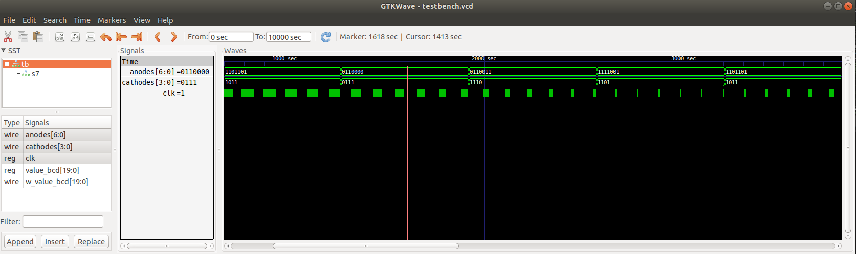 Figure 8: GTKWave simulation output for seven-segment display module
You can see that the anode and cathode values are consistent with the number displayed. The cathode cycles between the binary values 1110 to 0111 for each digit. The anode values match the digits. For example, 0110000 matches the digit “1”. Simulating the module helps us fix bugs easily during development!
Simulation of Binary to BCD Module
We will simulate the binary-to-BCD module by setting a binary value as input and verifying the output BCD value.
Here is the test bench code:
module tb ();

    reg clk = 0;

    initial begin
        $dumpfile("testbench.vcd");
        $dumpvars;
        #10000
        $finish;
    end

    reg [13:0] value = 9876;
    wire done;
    wire [19:0] value_bcd;

    bin_to_bcd bb1 (
        .clk(clk),
        .value_bin(value),
        .start(1'b1),
        .value_bcd(value_bcd),
        .done(done)
    );

    always @ (*) begin
        #5 clk <= ~clk;
    end

endmodule
We run the simulation using:
# make sim-b2b
iverilog -o tb.out -s tb testbench_b2b.v bin_to_bcd.v
vvp tb.out
gtkwave testbench.vcd
Here is the GTKWave output from the simulation:
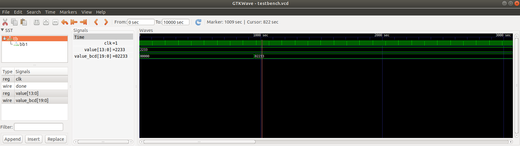 Figure 9: GTKWave simulation output for binary to BCD module
In Figure 9, you can see that the binary coded decimal value (represented in hexadecimal) matches the input value. Simulation is not just for checking the outputs — it is immensely helpful during development. When developing a state machine that implements the double dabble algorithm, it is crucial to be able to check if the state transitions happen as planned and if the values of internal registers are correct at each clock cycle.
Figure 10 shows how the internal registers change with the clock ticks:
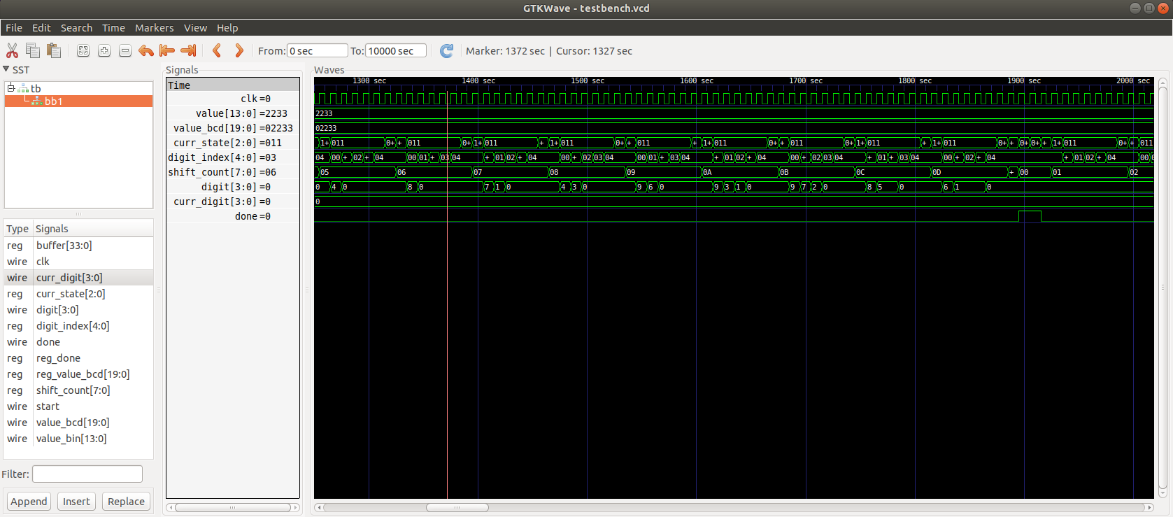 Figure 10: GTKWave simulation showing internal register states
And Figure 11 shows a zoomed-in version:
 Figure 11: GTKWave simulation — zoomed in view
GTKWave is a great interactive tool which lets you zoom in and out and observe the values of variables at any instant. I recommend running the simulation and going through the values of each internal register as the algorithm proceeds through its states. This will give you a clear understanding of how the binary to BCD conversion actually works.
FPGA Placement
Now that we’ve simulated the design, it’s time to fit it into our FPGA. For this, we will use the icestorm tools — yosys for synthesis, arachne-pnr for placement and routing, icepack to create the bitstream, and iceprog to upload the bitstream to the FPGA. Run make on the project and at the end you will see a report similar to the one below:
After placement:
PIOs  13 / 39
PLBs  115 / 660
BRAMs 0 / 30
...
write_txt ultrasonic.asc...
icepack ultrasonic.asc ultrasonic.bin
The report shows how much of the FPGA resources were taken up by our design: 13 out of 39 programmable IOs, 115 out of 660 available programmable logic blocks, and no Block RAM used. The result is a .bin file ready to be uploaded to the FPGA.
The icestorm tools output a large amount of debug information. It’s important to review it, as it helps with understanding what the tools are doing and with debugging. On Linux, you can capture both stdout and stderr to a text file:
make > out.txt 2>&1
In out.txt, look for warnings and errors. If your design doesn’t work, you’ll often find clues here — even if your simulation was fine.
To upload the bitstream to the FPGA:
sudo iceprog ultrasonic.bin
We use sudo for easy access to the hardware port. (You can also add your user to the correct group in Linux, e.g. dialout.) Here’s a typical output from iceprog:
init..
cdone: high
reset..
cdone: low
flash ID: 0x20 0xBA 0x16 0x10 0x00 0x00 0x23 0x74 0x21 0x42 0x03 0x00 0x52 0x00 0x12 0x06 0x12 0x17 0x64 0x63
file size: 104090
erase 64kB sector at 0x000000..
erase 64kB sector at 0x010000..
programming..
reading..
VERIFY OK
cdone: high
Bye.
Now it’s time to exercise the hardware we have created.
Hooking up the Hardware
Connect the display to the Lattice FPGA board as follows:
| Signal | FPGA Pin | Label on Board | Connection |
|---|---|---|---|
| A | 37 | 45A | Via 320 Ω resistor |
| B | 31 | 42B | Via 320 Ω resistor |
| C | 32 | 43A | Via 320 Ω resistor |
| D | 27 | 38B | Via 320 Ω resistor |
| E | 26 | 39A | Via 320 Ω resistor |
| F | 25 | 36B | Via 320 Ω resistor |
| G | 23 | 37A | Direct |
| D1 | 28 | 41A | Direct |
| D2 | 38 | 50B | Direct |
| D3 | 42 | 51A | Direct |
| D4 | 36 | 48B | Direct |
Do not connect pins A through F directly to the FPGA pins — connect them in series with 320 Ω resistors to limit current through the FPGA. (An alternate, more flexible solution is to use MOSFETs on each line, but that requires more components and wiring.)
Now connect the ultrasonic sensor as follows:
| Ultrasonic Sensor | FPGA Pin | Label on Board | Connection |
|---|---|---|---|
| VDD | — | — | To +5V supply |
| GND | GND | GND | Common ground |
| Echo | 43 | 49A | Via resistor divider |
| Trigger | 34 | 44B | Direct |
A small complication: the ultrasonic sensor requires 5V but our FPGA operates at 3.3V. The trigger signal is sent from the FPGA at 3.3V, so it poses no problem. But the echo signal comes in at 5V and that can damage the FPGA. A simple solution is to use a resistor divider as shown in Figure 12 to reduce the incoming signal to 3.3V. (A more elegant solution is a logic level translator, but since we have only one signal to worry about, the resistor divider works fine.)
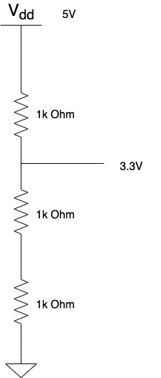 Figure 12: Resistor divider circuit for ultrasonic sensor echo line
In addition, the Lattice board does not have a 5V output. Use any external regulated 5V supply, and make sure the GND pin is connected to the GND of the FPGA board to establish a common ground reference.
Testing the Hardware
Enough with the theory! It’s now time to fire up our hardware and see if it works. Connect up the hardware as per the previous section. The arrangement should look more or less like Figure 13 below.
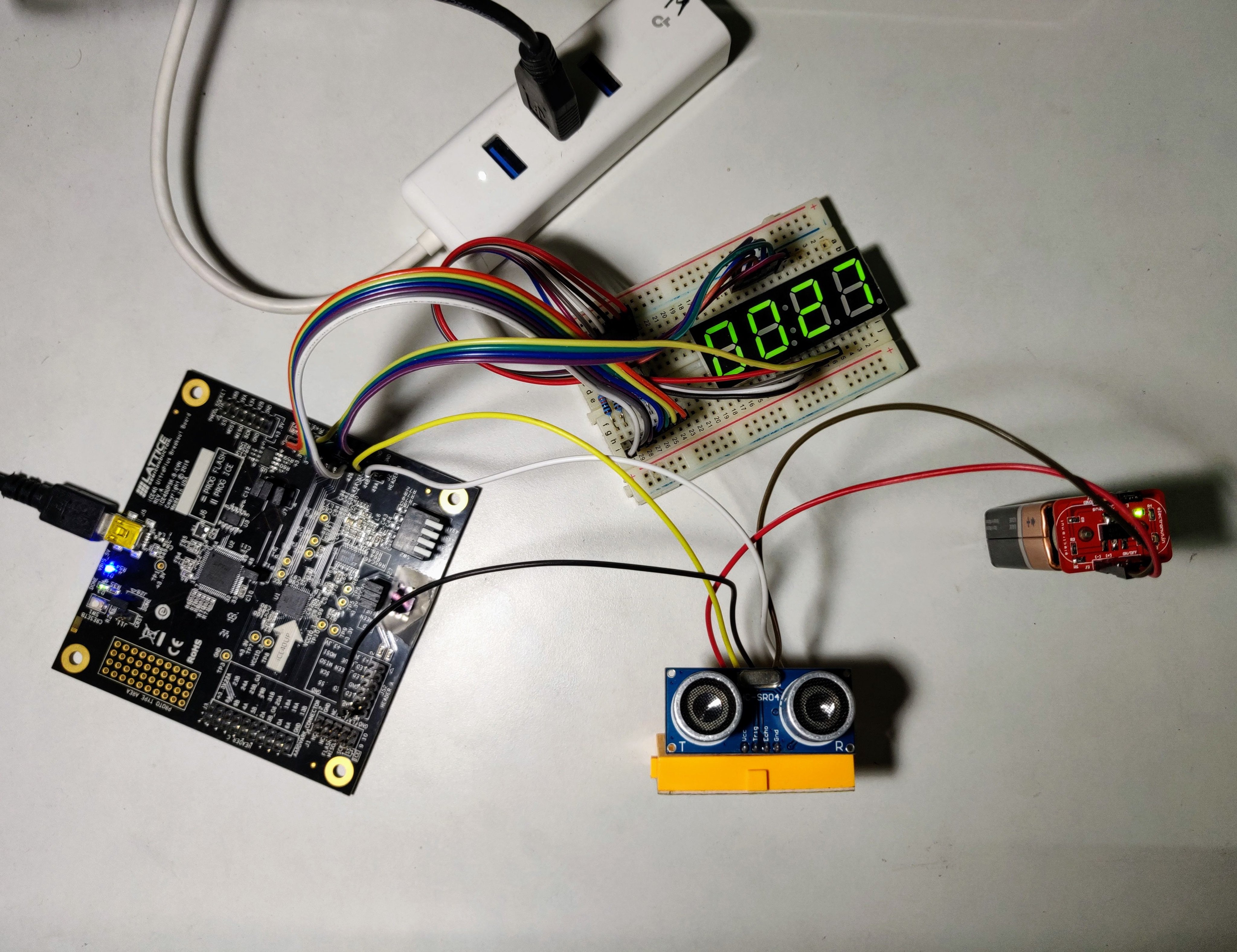 Figure 13: Photograph of completed hardware hookup
Place a flat object in front of the ultrasonic sensor. You should see the distance in centimeters on the display.
Code
The complete source code for this project is available on GitHub:
https://github.com/mkvenkit/learn_fpga/tree/main/ice40up5k/ultrasonic
Summary
In this project, we built an ultrasonic sensor display system that shows the distance from an object placed in front of the sensor. In this process, we built various Verilog modules for tasks such as edge detection, pulse width measurement, binary to BCD conversion, and driving a seven-segment display. Hopefully this article has given you a good insight into Verilog syntax and how you can design hardware on an FPGA.
Homework!
Now that you know how to display numbers from an FPGA, try to implement a stopwatch using the same display. You will need to hook up a couple of push buttons and 10kΩ resistors and connect them to the FPGA as shown in Figure 14 below.
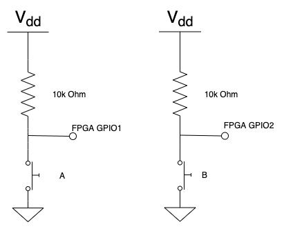 Figure 14: Push buttons for stopwatch
The stopwatch should function as follows: the display starts at zero. When you press button A, the display starts incrementing every one-hundredth of a second. Pressing button A while it’s running will pause the counter. Pressing B will reset the counter to zeros. The maximum time displayed will be 9999, or 99.99 seconds. (See if you can also get the decimal point to display — something we skipped in the main project!)
When you implement this, you may notice that button presses sometimes cause false starts and stops. This is because when you press a button, it can connect and reconnect a few times before it settles down, resulting in spurious intermediate signals. The solution to this problem is called debouncing. Read about it here and try to implement it in your stopwatch: